

 SMT(Surface Mount Technology) complies with the trend of miniaturization and lightness of intelligent electronic products, and lays a foundation for the realization of light, thin, short and small electronic products. SMT technology also came to maturity in the 1990s. However, with the rapid development of electronic products towards portable/miniaturized and networked direction, higher requirements are put forward for electronic assembly technology, among which BGA(Ball Grid Array) is a high-density assembly technology that has entered the practical stage.
The research on BGA technology began in the 1960s and was first adopted by IBM in the United States. However, it was not until the early 1990s that BGA really entered the stage of practical application. Due to the previous popular high-density pin device similar to QFP package, the limitation of its fine spacing is that the fine lead is easy to bend, brittle and easy to break, which requires high requirements for the co-planeness and mounting precision between the leads.
BGA technology is a new way of thinking in design. It USES a structure with circular or columnar points hidden under the package, with large lead spacing and short lead length. In this way, BGA eliminates the co-planeness and warping defects due to lead problems in finely spaced devices.
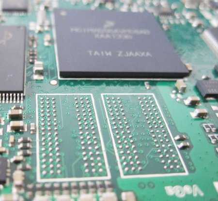
BGA is a commonly used component on A PCB, and usually 80% of high-frequency signals and special signals will be pulled from this type of package Footprint. Therefore, how to deal with the routing of BGA devices will have a great impact on important signals.
When wiring common BGA devices, the general steps are as follows:
Fan out and escape cabling is carried out according to applicable design rules. They include Fanout Control rules, routing width rules, routing through hole rules, routing layer rules and electrical spacing rules. If the rules are not set properly, such as the number of layers is not enough, the unlimited width is too wide to come out, the holes are too big to be punched, the spacing is illegal and the safe distance is not allowed, etc., fan out will fail.
When there is no response from the fan out operation, please check your various rule Settings and make appropriate modifications. The fan out can only be successful if there are no problems. The color of the thread is different for each layer.
The Fan out dialog box allows you to control and define options for fan out and escape wiring, and some options are for blind holes (holes between Layer pairs, which can be set in the Layer Stack Manager dialog box). Other options include whether to fan out the other two rows at the same time as the internal one, and whether only the pads assigned to the network are fan-out.
Due to its complex processing technology, in addition to its functional design, BGA mainly needs to communicate with PCB board making factory and SMT assembly factory in the design stage. Different manufacturers adopt different processes and have different capabilities. For processing and manufacturing costs, proofing and batch production are also different. Therefore, BGA design is more important to consider the processing cost, production yield rate and other factors.
Example:
This type of BGA module design has been the bottom line refresh, belongs to the category of minimum machining capacity. Let’s first take a look at its parameter characteristics:
BGA solder 0.3 mm (12 mil)
BGA center spacing is 0.4mm(16miL)
The X and Y directions of both pads and pads edge to edge are 0.1mm(4mil).
The diagonal direction of both pads and pads is 0.27mm(10.8mil).
Minimum linewidth: 0.1mm(4mil), minimum safety spacing: 0.1mm(4miL), minimum laser aperture: 0.1mm(4miL). We also do not consider mechanical drilling, laser holes are not fit!
 Question1: The line can’t come out!
— Solution: Blind buried hole drilling method instead of through hole
The minimum 4mil line width does not come out because the spacing is only 0.1mm(4mil). The BGA device in addition to the most outside a circuit can go out of the line, the inside of the line cannot be deployed out. So, it’s not possible to go Through holes, which at each layer block the wiring of the inner pads. Only blind buried hole can be used, and cross-layer perforated and cross-layer wired.
Question2: There is no place to punch the hole!
— Solution: Via in Pad
The minimum laser hole of 0.1mm(4mil) cannot be hit between the pads because the maximum diagonal spacing between the pads is 0.27mm. The smallest hole in the middle does not meet the safety rule of minimum spacing 4mil. Therefore, can only play plate hole. However, the process of disc hole is complex, which requires subsequent treatment, such as filling hole and plugging hole, adding electroplating, polishing surface, etc.
Processing costs will increase accordingly.
Technically can only carry out more than 4 layers of multilayer board wiring. The BGA device has a ball spacing of 0.4mm and a ball welding plate diameter of 0.3mm. Blind laser hole is needed for interconnection (the minimum machining aperture capacity of the laser is 0.1mm). Second-order interconnection is possible according to the design requirements. And need to do dish hole design.
During the design of PCB containing BGA components, in addition to the design on the technical and functional level, it is also necessary to communicate with the corresponding PCB manufacturer with such processing capability. Including manufacturing process and corresponding cost. Different processing technology will affect the difficulty of future packaging and paste, product yield.
After communication and consultation with the engineering and technical personnel of a board manufacturer (Shenzhen Renchuangyi Co., LTD.), the feedback information about the design, engineering design, processing technology and approximate cost of the PCB containing this small-spacing BGA device is as follows.
In terms of processing technology, the laser blind hole process requires VCP side spraying pulse electroplating copper to fill the blind hole, and after grinding, negative acid etching is done to ensure the integrity of BGA. After etching, the final size of BGA is 0.27mm~0.28mm.
In addition, due to the small BGA spacing, processing needs to pay attention to matters;
XPCB Limited is a premium PCB & PCBA manufacturer based in China.
We specialize in multilayer flexible circuits, rigid-flex PCB, HDI PCB, and Rogers PCB.
Quick-turn PCB prototyping is our specialty. Demanding project is our advantage.
Tel : +86-136-3163-3671
Fax : +86-755-2301 2705
Email : [email protected]
© 2023 - XPCB Limited All Right Reserve
