

 PCB manufacturing is now at the heart of current global technology trends. Every other day, electronic instruments and components demonstrate the pace of innovation as technology advances rigorously, as global market trends become dynamic, and as customer preferences and demands for unique electronic products change.
Even in the case of complex critical PCB layout requirements, this is an issue of equal concern to electronics manufacturers and PCB manufacturers for reliable, high quality, low cost electronic solutions.
A recent growth trend in PCB manufacturing is the use of heavy copper in PCB manufacturing.
When we talk about printed circuit boards, they have applications in every aspect of human life. From telecommunications, healthcare, automotive, defense, aerospace, military to renewable energy, transportation, industrial sector and many other leading industries.
On the other hand, the demand for faster, compact, safe product use as well as higher efficiency and high-power performance of high-tech electronic machinery and electrical appliances is the customer’s desire to introduce new technologies every other day.
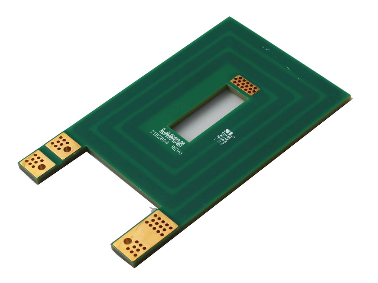
This makes the PCB industry a leader in innovation and transformation. Regardless of heat dissipation, speed, high frequency or other key design requirements, heavy copper in PCB manufacturing has a high-performance output. Printed circuit boards made of heavy copper consist of a fine combination of copper electroplating and copper etching. As thin copper foil, these layers are made from electrical circuits.
In addition, copper etching enables the elimination of unwanted copper and copper plating techniques, thereby optimizing the copper thickness of trace lines, pads, surfaces, and boreholes on circuit boards. Epoxy substrates are used to complete the final lamination of the middle layer of the circuit board.These heavy copper PCBS are made from thermal layers and are best suited for multi-layer PCBS.
In short, heavy copper PCBS are made from the manufacture of high finished copper in the internal and external substrates of the circuit board, also known as cascading deposits.
Another major reason for the high usage of heavy copper PCBS is the reduction in extremely complex wired bus configurations.
With these abundant heavy copper PCBS, researchers are working toward effective ways to implement unique PCB layouts to meet complex requirements, make them more cost-effective, and provide high quality PCB manufacturing.
Printed circuit boards (PCBS) are usually coated with copper foil of 18 m, 35 m, 55 m and 70 m thickness on glass epoxy substrate. The most commonly used copper foil is 35 m thick. Copper foil thickness is generally 35~50 m, there are thinner than this such as 10 m, 18 m; And thicker than that like 70 m.
The thickness of composite copper foil on a L ~3mm thick substrate is about 35 m; The thickness of composite copper foil on a substrate less than LMM thick is about 18 m, and the thickness of composite copper foil on a substrate more than 5mm is about 55 m.
If the PCB thickness of copper foil is 35 microns, printed line 1 mm wide, each 10 mm long, its resistance is about 5 m Ω, its inductance for 4nh or so. When the di/dt of the digital integrated circuit chip on the PCB is 6mA/ns and the working current is 30mA, the noise voltage generated by each part of the circuit is estimated by the resistance and inductance values contained in each 10mm long printed line as 0.15mv and 24mV respectively.
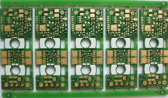
Product types: single-sided, double-sided and multi-layer printed circuit board (PCB), flexible (soft) circuit board, buried blind hole board.
Maximum processing size: single panel, double panel: 1000mm * 600mm Multilayer panel: 600mm * 600mm
Layer: 20 L
Board thickness: rigid 0.4mm -4.0mm flexible 0.025mm– 0.15mm
Thickness of copper foil base: rigid plate 18 (1/2 oz),35 (1OZ),70 (2OZ) flexible plate 0.009MM 0.018 MM 0.035 MM 0.070 MM 0.010 MM
(1) Drilling: the minimum aperture is 0.15mm
(2) Hole metallization: minimum aperture 0.15mm, plate thickness/aperture ratio 4:1
(3) Wire width: Minimum wire width: gold plate 0.075mm, tin plate 0.10mm
(4) Wire spacing: Minimum spacing: gold plate 0.075mm, tin plate 0.10mm
(5) gold-plated plate: nickel layer thickness: > or =2.5 gold layer thickness: 0.05-0.1 m or according to customer requirements
(6) HASL plate: Tin thickness: & GT; Or = 2.5 5 mu
(7) Milling plate: Minimum distance from line to edge: 0.15mm Minimum distance from hole to edge: 0.2mm minimum contour tolerance: ± 0.12mm
(8) Socket chamfering: Angle: 30 degrees, 45 degrees, 60 degrees Depth: 1-3mm
(9) V cut: Angle: 30 degrees, 35 degrees, 45 degrees Depth: plate thickness 2/3 Minimum size: 80mm * 80mm
(10) On-off test: Welding resistance :85– 105℃ / 280℃– 360℃. Flexural/chemical resistance of flexible plate: in full compliance with international standards
XPCB Limited is a premium PCB & PCBA manufacturer based in China.
We specialize in multilayer flexible circuits, rigid-flex PCB, HDI PCB, and Rogers PCB.
Quick-turn PCB prototyping is our specialty. Demanding project is our advantage.
Tel : +86-136-3163-3671
Fax : +86-755-2301 2705
Email : [email protected]
© 2023 - XPCB Limited All Right Reserve
