• +86-755-23012705
  • [email protected]
  • Building 3, Jinfeng Industrial Park, Fuyong Street, Baoan District, Shenzhen ,China
Search
Close
logo
  • Home
  • About Us
    • About XPCB
    • Flexible PCB Fabrication
    • PCB Fab Capability
    • PCBA Capability
    • Our Certifications
    • Our Facility
    • Quality Assurance
  • PCB Fabrication
    • Flexible PCB
    • Rigid Flex PCB
    • Rigid PCB
    • ELIC HDI PCB
    • RF PCB
    • Medical PCB
    • Automotive PCB
    • IoT & IIoT PCB
    • Industrial Control PCB
    • Telecommunication PCB
    • Consumer Electronics PCB
  • PCB Assembly
    • Turn Key PCB Assembly
    • Consigned PCB Assembly
    • Components Sourcing
  • Resources
    • PCB Glossary
    • PCB Design Guide
    • PCB Blog
  • Contact
Menu
  • Home
  • About Us
    • About XPCB
    • Flexible PCB Fabrication
    • PCB Fab Capability
    • PCBA Capability
    • Our Certifications
    • Our Facility
    • Quality Assurance
  • PCB Fabrication
    • Flexible PCB
    • Rigid Flex PCB
    • Rigid PCB
    • ELIC HDI PCB
    • RF PCB
    • Medical PCB
    • Automotive PCB
    • IoT & IIoT PCB
    • Industrial Control PCB
    • Telecommunication PCB
    • Consumer Electronics PCB
  • PCB Assembly
    • Turn Key PCB Assembly
    • Consigned PCB Assembly
    • Components Sourcing
  • Resources
    • PCB Glossary
    • PCB Design Guide
    • PCB Blog
  • Contact
Get Instant Quote

Introduction To High Frequency PCB Material and How To Process It

1. Definition of PCB high-frequency board


High-frequency board refers to the special electromagnetic frequency circuit board, used in high frequency (greater than 300 MHZ frequency or wavelength is less than 1 meter) and microwave (greater than 3 GHZ frequency or wavelength is less than 0.1 meters) in the field of PCB, is on the microwave base copper clad using common rigid circuit board manufacturing method of a part of the process or the use of special processing methods and the production of circuit boards. In general, a high-frequency board can be defined as a circuit board with a frequency of more than 1GHz.

With the rapid development of science and technology, more and more equipment designs are applied in microwave frequency band (> 1GHZ) and even above the millimeter wave field (30GHZ), which also means that the frequency is getting higher and higher, and the requirements on the base material of circuit board are also getting higher and higher. For example, the substrate material needs to have excellent electrical performance, good chemical stability, with the increase of the power signal frequency on the substrate loss requirements are very small, so the importance of high-frequency plate protrudes out.


2. Application field of PCB high-frequency board


2.1 Mobile communication products

2.2 Power amplifier, low noise amplifier, etc

2.3 Passive devices such as power dividers, couplers, diplexers, filters, etc

2.4 Automobile anti-collision system, satellite system, radio system and other fields.

High frequency of electronic equipment is the development trend.


3. Classification of high frequency boards


3.1 Powder ceramic filled thermosetting material

Manufacturer:

Rogers 4350B/4003C

25N/25FR for Arlon

Taconic’s TLG series


Processing method:

Similar to epoxy/glass woven fabric (FR4), but the plates are brittle and easily broken. The life of drill tip and gongs is reduced by 20% for drilling and routing.


3.2 PTFE(Teflon) material


A: The manufacturer

Rogers RO3000 series, RT series, TMM series

Arlon’s AD/AR series, IsoClad series, CuClad series

Taconic RF series, TLX series, TLY series

F4B, F4BM, F4BK and TP-2 of Taixing microwave

B: Processing method

  • Material opening: The protective film must be kept to prevent scratch and indentation
  • The drill:
  • Use new drill heads (standard 130), block by block is the best, the foot pressure is 40psi
  • The aluminum sheet is the cover plate, and then the PTFE plate is tightened with 1mm dense amine backing plate
  • After drilling, use the air gun to blow the dust out of the hole
  • Use the most stable drill and drill hole parameters (basically, the smaller the hole, the faster the drilling rate; the smaller the Chip load, the smaller the recovery rate)
  • The hole processing: Plasma treatment or sodium naphthalene activation treatment facilitates metallization of pores
  • PTH sink copper
  • After micro etching (controlled by micro etching rate of 20 microinch), pull from the oil cylinder to enter the plate at PTH
  • If necessary, pass the second PTH, only from the expected? The cylinder begins to feed
  • The soldermask
  • Pretreatment: Acid washing plate shall be used instead of mechanical grinding plate
  • After pretreatment, the curing plate (90℃, 30min) is brushed with green oil for curing
  • Divided into three sections: one section at 80 ° c, 100 ° c and 150 ° c for 30min each (if oil is dumped on the substrate surface, it can be reworked: wash off the green oil and re-activate the treatment)
  • Routing: Lay the white paper on the line surface of PTFE board, and clamp it up and down with FR-4 substrate or phenolic substrate etched with a thickness of 1.0mm to remove copper: as shown in the figure:

High frequency plate stact up Introduction To High Frequency PCB Material and How To Process It

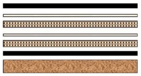
High-frequency plate routing plate lamination method

After the routing, the board edge burrs need to be carefully scraped by hand, to prevent damage to the substrate and copper surface, and then use the appropriate size of sulfur-free paper separation, and visual detection, to reduce burrs, the key is the gongs process to the effect of good.


4. Process flow


4.1. PTFE plate processing process of NPTH


Material opening – drilling – dry film – inspection – etching – corrosion inspection – welding resistance – character – spray tin – molding – test – final inspection – packaging – shipment


4.2. PTFE plate processing process of PTH


Material opening – drilling – hole treatment (plasma treatment or sodium naphthene activation treatment)- immersed copper – plate electricity – dry film – inspection – graphic electricity – etching – welding resistance – character – spray tin – forming – test – final inspection – packaging – shipment


Summary: high frequency plate processing difficulties


  • Sink copper: it is not easy to put copper on the hole wall
  • Control of drawing, etching, line width gap and sand hole
  • Green oil process: green oil adhesion, green oil bubbling control
  • Strictly control board surface scratches in each process, etc

H F pcb Introduction To High Frequency PCB Material and How To Process It


Request Quote for Your PCB Now
Share
amazon
amphenol-logo
halliburton
intel logo
samtec logo
sanmina logo
Previous
Next

Company Info

XPCB Limited is a premium PCB & PCBA manufacturer based in China.

We specialize in multilayer flexible circuits, rigid-flex PCB, HDI PCB, and Rogers PCB.

Quick-turn PCB prototyping is our specialty.  Demanding project is our advantage.

Head Office

XPCB Limited
Address :
Building 3, JinFeng Industry Area,  Fuyong Town, Baoan District, Shenzhen, Guangdong, 518103, China.

Tel : +86-136-3163-3671
Fax : +86-755-2301 2705
Email : [email protected]

Quick Links

  • Flexible PCB
  • Rigid Flex PCB
  • ELIC HDI PCB
  • RF PCB
  • PCB Capability
  • PCBA Capabiility
  • About Us

PCB Blog

Electromagnetic Compatibility Design of Mobile Phone PCB (1)

Read More »

The PCB Circuit Design of LED Switching Power Supply

Read More »

Electromagnetic Compatibility Design of Mobile Phone PCB (2)

Read More »

© 2023 - XPCB Limited All Right Reserve