• +86-755-23012705
  • Building 3, Jinfeng Industrial Park, Fuyong Street, Baoan District, Shenzhen ,China
  • [email protected]
logo
  • Home
  • About Us
    • Flexible PCB Expertise
    • Our Certifications
    • Our Facility
    • Quality Assurance
  • PCB Fabrication
    • Flexible PCB
    • Rigid Flex PCB
    • Rigid PCB
    • ELIC HDI PCB
    • RF PCB
    • Medical PCB
    • Automotive PCB
    • IoT & IIoT PCB
    • Industrial Control PCB
    • Telecommunication PCB
    • Consumer Electronics PCB
  • PCB Assembly
    • Turn Key PCB Assembly
    • Consigned PCB Assembly
    • Components Sourcing
  • Capabilities
    • PCB Fab Capability
    • ATE PCB Fabrication
    • PCB Technology Roadmap
    • PCB Assembly Services
    • PCB Design Support
  • Contact
  • Resources
    • PCB Blog
    • PCB Glossary
Get Quote

Optimizing PCBA Service Processes: Solutions Based on HDI PCB and Blind/Buried Via Design

Microvia Aspect Ratio Optimizing PCBA Service Processes: Solutions Based on HDI PCB and Blind/Buried Via Design

The evolution of electronic devices has propelled advancements in Printed Circuit Board Assembly (PCBA) services. As the demand for compact, efficient, and high-performance electronics increases, the integration of High-Density Interconnect (HDI) PCBs and the strategic use of blind via and buried via designs have become essential. These technologies streamline PCBA processes, enhance product quality, and address the growing complexities of modern electronic systems. In this blog, we explore how HDI PCBs and advanced via designs optimize PCBA service processes.


The Role of HDI PCBs in Modern Electronics

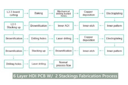
High-Density Interconnect (HDI) PCBs are characterized by their fine lines, small vias, and high component density. They support intricate designs and advanced functionalities, making them indispensable for industries like consumer electronics, automotive, medical devices, and aerospace. The key features of HDI PCBs include:

  • Microvias: These enable efficient interconnections between layers.
  • Thin Dielectric Layers: Allowing close stacking of layers for compact designs.
  • High Signal Integrity: Reducing signal loss and interference.
  • Improved Thermal Management: Ensuring reliability in high-performance devices.

These characteristics directly impact PCBA processes by offering enhanced design flexibility and facilitating the integration of complex components.


Blind and Buried Vias: Cornerstones of HDI Design

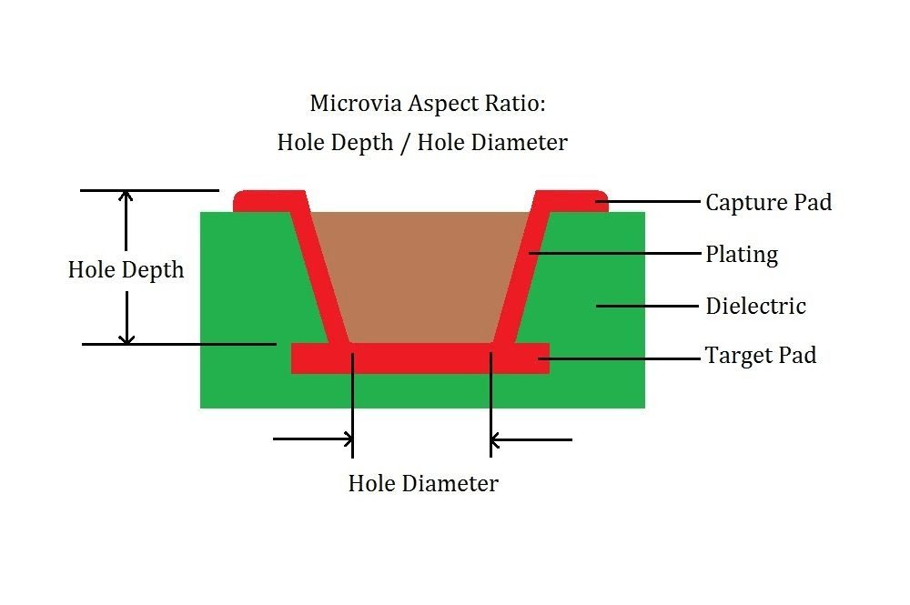
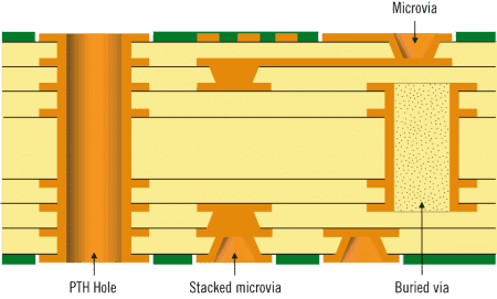
Blind vias and buried vias are essential design elements in HDI PCBs, contributing significantly to their functionality:

  • Blind Vias: Connect an outer layer to one or more inner layers without penetrating through the entire board. They save surface space for components and routing.
  • Buried Vias: Connect internal layers without reaching the outer layers, further optimizing layer-to-layer connectivity without affecting surface design.

These via types enable efficient multilayer designs, reducing the overall size of PCBs while maintaining functionality. They also play a critical role in minimizing signal interference and improving electrical performance.


HDI PCB manufacturer stackup


Optimizing PCBA Processes with HDI and Advanced Vias

1. Enhanced Design and Layout Efficiency

The compact nature of HDI PCBs with blind and buried vias allows engineers to achieve intricate designs with reduced board size. This efficiency minimizes the need for extensive routing and enhances the assembly process, resulting in faster production cycles.

2. Streamlined Component Placement

The additional surface space made available by blind vias facilitates the placement of more components or larger chips. Automated assembly equipment can place these components with higher precision, reducing errors and rework.

3. Improved Signal Performance

By reducing the distance between layers and minimizing via lengths, HDI designs with blind and buried vias enhance signal integrity. This capability is crucial for high-frequency applications where signal degradation can compromise functionality.

4. Reduced Manufacturing Complexity

Advanced via technologies simplify the layer-to-layer connection process, reducing the overall complexity of PCB manufacturing. This simplification translates into more efficient PCBA workflows and cost savings.

5. Superior Thermal Management

Blind and buried vias can serve as thermal conduits, dissipating heat more effectively from critical areas. This feature ensures stable operation, particularly in high-power devices, and minimizes the risk of component failure.


Applications Benefiting from HDI and Advanced Vias

Several industries benefit from the integration of HDI PCBs and blind/buried via designs in PCBA processes:

  • Consumer Electronics: Devices like smartphones, tablets, and wearables rely on HDI designs for their compactness and functionality.
  • Automotive: Advanced Driver Assistance Systems (ADAS) and infotainment systems require high-performance PCBs with efficient signal integrity and heat management.
  • Medical Devices: Miniaturized diagnostic tools and implantable devices depend on the reliability and precision of HDI technology.
  • Aerospace and Defense: High-density and high-reliability designs are crucial for mission-critical applications.


HDI PCB FABRICATION PROCESS


Challenges and Solutions


Challenges:

  • Manufacturing Complexity: HDI PCBs and advanced via designs demand precise manufacturing processes.
  • Cost Considerations: Initial production costs for HDI boards with blind and buried vias are higher.


Solutions:

  • Advanced Manufacturing Equipment: Investing in cutting-edge laser drilling and plating technologies ensures precision and reduces defects.
  • Design Optimization Tools: Utilizing CAD software tailored for HDI and via design streamlines the development process.
  • Partnering with Experienced Providers: Collaborating with seasoned PCBA service providers ensures quality and efficiency in handling advanced designs.


HDI PCB benefits


Conclusion

The integration of HDI PCBs and blind/buried via designs revolutionizes PCBA service processes by addressing the complexities of modern electronic systems. From enhancing design flexibility to improving signal performance and thermal management, these technologies offer comprehensive solutions for high-performance applications. As industries continue to demand more from electronic devices, adopting HDI technology and advanced via designs will be pivotal in meeting these challenges and driving innovation forward.


XPCB Limited: Your One-Stop Solution for PCB Manufacturing and Assembly


XPCB Limited is your one-stop solution for all your PCB manufacturing and assembly needs. From design and prototyping to full-scale production, we offer comprehensive services under one roof. With a focus on quality, efficiency, and customer satisfaction, we make it easy for you to complete your projects with confidence. Simplify your PCB process today with XPCB Limited.

Share

Related posts

dispensing in PCB
2025-02-07

Multilayer PCB Assembly and HDI PCB Manufacturing for High-Tech Solutions


Read more
smt product line
2025-02-06

Streamline Your PCB Production with XPCB’s Turnkey PCBA Services


Read more
2025-02-05

Comprehensive Turnkey PCBA Services: From BOM to SMT Assembly


Read more
amazon
amphenol-logo
halliburton
intel logo
samtec logo
sanmina logo

Company Info

XPCB Limited is a premium PCB & PCBA manufacturer based in China.

We specialize in multilayer flexible circuits, rigid-flex PCB, HDI PCB, and Rogers PCB.

Quick-turn PCB prototyping is our specialty.  Demanding project is our advantage.

Head Office

XPCB Limited
Address :
Building 3, JinFeng Industry Area,  Fuyong Town, Baoan District, Shenzhen, Guangdong, 518103, China.

Tel : +86-136-3163-3671
Fax : +86-755-2301 2705
Email : [email protected]

Quick Links

  • Flexible PCB
  • Rigid Flex PCB
  • ELIC HDI PCB
  • RF PCB
  • PCB Capability
  • PCBA Capabiility
  • About Us

PCB Blog

Multilayer PCB Assembly and HDI PCB Manufacturing for High-Tech Solutions

Read More »

Streamline Your PCB Production with XPCB’s Turnkey PCBA Services

Read More »

Comprehensive Turnkey PCBA Services: From BOM to SMT Assembly

Read More »

© 2024 - XPCB Limited All Right Reserve