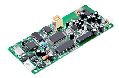
Printed Circuit Boards (PCBs) are the backbone of modern electronic devices, providing the framework for electrical connections and supporting various components. As the demand for smaller, more powerful, and efficient devices grows, PCB manufacturing has undergone significant advancements. Among these, High-Density Interconnect (HDI) technology and the use of blind and buried vias stand out as transformative innovations. This blog explores the future of complex PCB manufacturing, focusing on these critical technologies and their developments.
The Rise of HDI Technology
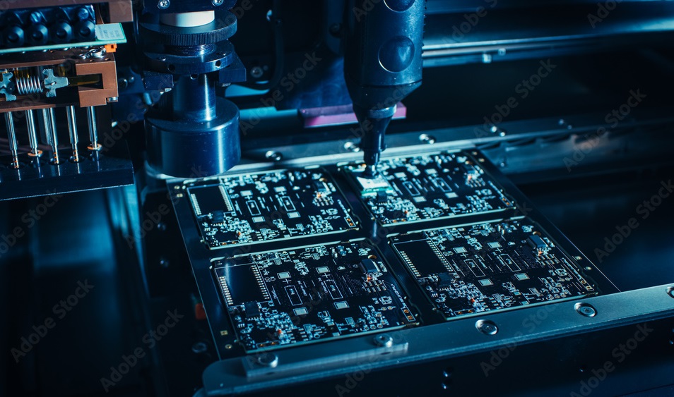
HDI PCBs are characterized by their higher wiring density per unit area compared to traditional PCBs. They achieve this through microvias, finer lines and spaces, and thinner materials. These features make HDI an essential technology for advanced applications in smartphones, wearables, medical devices, and automotive electronics.
Current Trends in HDI Technology
- Miniaturization: The ongoing trend toward smaller and lighter electronic devices drives the need for compact HDI designs. HDI enables the integration of more functionality within a limited space by accommodating finer traces and denser components.
- Layer Stacking: Modern HDI boards often employ multiple layers with microvias that can connect components through various depths. This capability supports complex and high-performance designs required for applications like 5G and AI computing.
- Materials Innovation: Advanced materials with superior thermal and electrical properties are being developed to meet the stringent demands of HDI PCBs. For example, low-loss laminates improve signal integrity in high-speed applications.
Future Prospects for HDI
The future of HDI technology lies in further enhancing performance while reducing costs. Automation and AI in design and manufacturing processes are set to improve production efficiency. Additionally, emerging applications, such as foldable devices and IoT sensors, will continue to push the boundaries of HDI innovation.
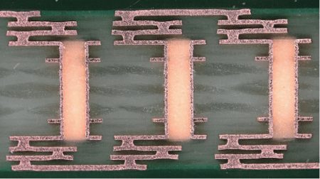
Blind and Buried Vias: Unlocking Complexity
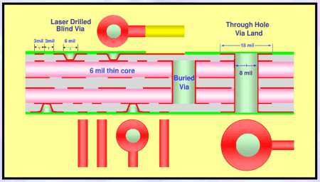
Blind and buried vias are essential features of complex PCBs, enabling connections between layers without occupying surface area. A blind via connects an outer layer to one or more inner layers, while a buried via connects only inner layers.
Innovations in Via Technologies
- Laser Drilling: Laser technology has revolutionized via creation by enabling precise and consistent drilling of microvias. This method is critical for HDI designs, where traditional mechanical drilling cannot achieve the necessary accuracy.
- Via-in-Pad Designs: This approach integrates vias directly into component pads, optimizing space and improving signal integrity. It is particularly beneficial in high-speed and high-frequency circuits.
- Conductive Fill Materials: Advances in conductive epoxy and copper filling materials have improved the reliability and performance of blind and buried vias, making them more suitable for demanding applications.
Challenges and Opportunities
While blind and buried vias enhance PCB design flexibility, they also pose challenges such as higher manufacturing complexity and costs. However, innovations like improved drilling techniques and materials are gradually addressing these issues. As the industry adopts new standards and processes, these vias are expected to become more accessible for a broader range of applications.
The Convergence of HDI and Advanced Via Technologies
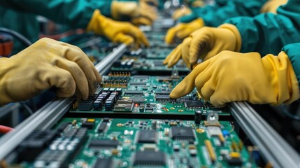
The integration of HDI and blind/buried via technologies is creating opportunities for increasingly complex PCB designs. Together, they enable higher functionality, better signal integrity, and greater reliability in compact electronic devices. Industries such as aerospace, defense, and telecommunications are at the forefront of leveraging these advancements for cutting-edge applications.
Sustainability and Eco-Friendly Practices
As the PCB industry evolves, sustainability is becoming a critical focus. Manufacturers are exploring eco-friendly materials, reducing waste in production processes, and improving recycling methods. These practices are crucial in ensuring that the rapid advancement of technologies like HDI and advanced vias does not come at an unsustainable environmental cost.
Conclusion
The future of complex PCB manufacturing is bright, driven by continuous innovations in HDI and blind/buried via technologies. These advancements are shaping a new era of electronics, characterized by higher performance, miniaturization, and versatility. As manufacturers embrace cutting-edge techniques and materials, the potential for more sophisticated and eco-friendly electronic devices will only grow. The convergence of these technologies not only supports the demands of modern industries but also paves the way for groundbreaking innovations in the years to come.
Advanced PCB Manufacturing and Quick-Turnaround Prototyping by XPCB Limited
XPCB Limited specializes in delivering advanced PCB manufacturing combined with quick-turnaround prototyping to meet the demands of your most time-sensitive projects. With cutting-edge technology and a commitment to precision, we provide exceptional PCB solutions tailored to your specifications. Trust XPCB Limited to help you accelerate your development cycle without compromising on quality.