• +86-755-23012705
  • [email protected]
  • Building 3, Jinfeng Industrial Park, Fuyong Street, Baoan District, Shenzhen ,China
Search
Close
logo
  • Home
  • About Us
    • About XPCB
    • PCB Capability
    • PCBA Capability
    • Our Certifications
    • Our Facility
    • Quality Assurance
  • PCB Fabrication
    • Rigid PCB
    • Rigid Flex PCB
    • Flexible PCB
    • ELIC HDI PCB
    • RF PCB
    • Medical
    • Industrial Control
    • IoT & IIoT
    • Telecommunication
    • Automotive
    • Consumer Electronics
  • PCB Assembly
    • Turn Key PCB Assembly
    • Consigned PCB Assembly
    • Components Sourcing
  • Resources
    • PCB Glossary
    • PCB Design Guide
    • PCB Blog
  • Contact
Menu
  • Home
  • About Us
    • About XPCB
    • PCB Capability
    • PCBA Capability
    • Our Certifications
    • Our Facility
    • Quality Assurance
  • PCB Fabrication
    • Rigid PCB
    • Rigid Flex PCB
    • Flexible PCB
    • ELIC HDI PCB
    • RF PCB
    • Medical
    • Industrial Control
    • IoT & IIoT
    • Telecommunication
    • Automotive
    • Consumer Electronics
  • PCB Assembly
    • Turn Key PCB Assembly
    • Consigned PCB Assembly
    • Components Sourcing
  • Resources
    • PCB Glossary
    • PCB Design Guide
    • PCB Blog
  • Contact
Get Instant Quote

PCB Through Hole Plating Steps (2)

3. PCB Electroplating:

3.1 Immerse the PCB in the water tank or flush it directly, so that the wall of the hole can be fully wetted. After wetting, pay attention that there are no air bubbles in the wall of the hole. If there are air bubbles, flush them with water to remove them.

3.2 Put the PCB into the electroplating tank, and shake the PCB back and forth in the tank (about 10 times) to completely wet the hole wall with the plating solution.

3.3 Use a dovetail clip to fix it in the center of the slot. Taking an A4 size PCB as an example, the plating current is 3.5A, and the plating time is 60 minutes.

*In order to obtain better electroplating quality, it is best to place the board in the center of the electroplating tank, and the alligator clip (black) of the cathode is clamped in the center of the crossbar, so that the concentration of the electroplating solution and the electroplating current can be evenly distributed to each part of the PCB, and get better plating quality.

3.4 The PCB plating current setting ratio is recommended to set the current according to the size of the PCB.

3.5 After the electroplating is completed, take out the PCB, rinse it with clean water and then dry it to avoid oxidation on the surface of the PCB.

3.6 After the electroplating is completed, use 400-grit fine sandpaper or steel wool to grind the surface of the PCB comprehensively back and forth until the surface of the PCB is smooth, so as to level the bumps and depressions generated during electroplating to avoid errors in plane detection during PCB engraving.

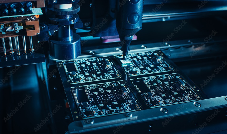
3.7 Move the board to the PCB engraving machine for circuit fabrication.

Share

Related posts

2022-05-20

Electromagnetic Compatibility Design of Mobile Phone PCB (2)


Read more
2022-05-20

Electromagnetic Compatibility Design of Mobile Phone PCB (1)


Read more
2022-05-20

The PCB Circuit Design of LED Switching Power Supply


Read more
amazon
amphenol-logo
halliburton
intel logo
samtec logo
sanmina logo
Previous
Next

Company Info

XPCB Limited is a premium PCB & PCBA manufacturer based in China.

We specialize in multilayer flexible circuits, rigid-flex PCB, HDI PCB, and Rogers PCB.

Quick-turn PCB prototyping is our specialty.  Demanding project is our advantage.

Head Office

XPCB Limited
Address :
Building 3, JinFeng Industry Area,  Fuyong Town, Baoan District, Shenzhen, Guangdong, 518103, China.

Tel : +86-136-3163-3671
Fax : +86-755-2301 2705
Email : [email protected]

Quick Links

  • Flexible PCB
  • Rigid Flex PCB
  • ELIC HDI PCB
  • RF PCB
  • PCB Capability
  • PCBA Capabiility
  • About Us

PCB Blog

Electromagnetic Compatibility Design of Mobile Phone PCB (1)

Read More »

The PCB Circuit Design of LED Switching Power Supply

Read More »

Electromagnetic Compatibility Design of Mobile Phone PCB (2)

Read More »

© 2022 - XPCB Limited All Right Reserved