• +86-755-23012705
  • Building 3, Jinfeng Industrial Park, Fuyong Street, Baoan District, Shenzhen ,China
  • [email protected]
logo
  • Home
  • About Us
    • Flexible PCB Expertise
    • Our Certifications
    • Our Facility
    • Quality Assurance
  • PCB Fabrication
    • Flexible PCB
    • Rigid Flex PCB
    • Rigid PCB
    • ELIC HDI PCB
    • RF PCB
    • Medical PCB
    • Automotive PCB
    • IoT & IIoT PCB
    • Industrial Control PCB
    • Telecommunication PCB
    • Consumer Electronics PCB
  • PCB Assembly
    • Turn Key PCB Assembly
    • Consigned PCB Assembly
    • Components Sourcing
  • Capabilities
    • PCB Fab Capability
    • ATE PCB Fabrication
    • PCB Technology Roadmap
    • PCB Assembly Services
    • PCB Design Support
  • Contact
  • Resources
    • PCB Blog
    • PCB Glossary
Get Quote

PCB Circuit Board Copper Clad Processing

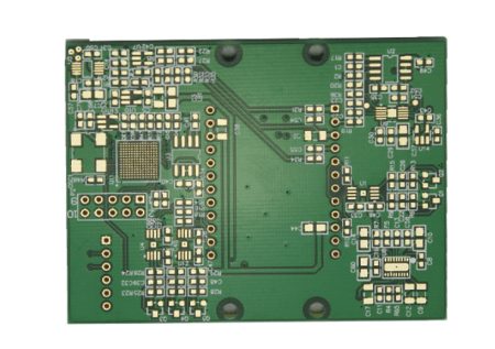
Copper pour is to use the unused space on the PCB as a reference surface and then fill it with solid copper. These copper areas are also called copper filling. The significance of copper coating is to reduce the bottom line impedance, improve the anti-interference ability, reduce the voltage drop, improve the power efficiency, and connect to the ground wire to reduce the loop area. If the PCB has a lot of ground, such as SGND, AGND, GND, how to pour copper? According to the position of the PCB board, the main bottom line is used as the reference to pour copper independently, and the digital ground and analog ground are separated to pour copper. At the same time, before the copper pour, first thicken the corresponding power connection: V5.0V, V3.6V, V3.3V (SD card power supply), etc., in this way, a plurality of polygonal structures with different shapes are formed.

PCB Circuit Board Copper Clad Processing PCB Circuit Board Copper Clad Processing

There are several problems to be dealt with in copper coating: one is the single-point connection to different grounds, and the other is the copper coating near the crystal oscillator. The crystal oscillator in the circuit is a high-frequency emission source. The method is to surround the crystal oscillator with copper and then ground the crystal oscillator separately. The third is the island (dead zone) problem, you can define a ground via to add it.

In addition, it is impossible to say whether large-area copper pour is better or network copper pour is better. For large area copper plating, if wave soldering is used, the board may be uplifted or even blistered. From this point of view, the grid has better heat dissipation. Generally, high-frequency circuits require high multi-purpose grids, and low-frequency circuits have high-current circuits and other commonly used complete copper coatings.

Share

Related posts

dispensing in PCB
2025-02-07

Multilayer PCB Assembly and HDI PCB Manufacturing for High-Tech Solutions


Read more
smt product line
2025-02-06

Streamline Your PCB Production with XPCB’s Turnkey PCBA Services


Read more
2025-02-05

Comprehensive Turnkey PCBA Services: From BOM to SMT Assembly


Read more
amazon
amphenol-logo
halliburton
intel logo
samtec logo
sanmina logo

Company Info

XPCB Limited is a premium PCB & PCBA manufacturer based in China.

We specialize in multilayer flexible circuits, rigid-flex PCB, HDI PCB, and Rogers PCB.

Quick-turn PCB prototyping is our specialty.  Demanding project is our advantage.

Head Office

XPCB Limited
Address :
Building 3, JinFeng Industry Area,  Fuyong Town, Baoan District, Shenzhen, Guangdong, 518103, China.

Tel : +86-136-3163-3671
Fax : +86-755-2301 2705
Email : [email protected]

Quick Links

  • Flexible PCB
  • Rigid Flex PCB
  • ELIC HDI PCB
  • RF PCB
  • PCB Capability
  • PCBA Capabiility
  • About Us

PCB Blog

Multilayer PCB Assembly and HDI PCB Manufacturing for High-Tech Solutions

Read More »

Streamline Your PCB Production with XPCB’s Turnkey PCBA Services

Read More »

Comprehensive Turnkey PCBA Services: From BOM to SMT Assembly

Read More »

© 2024 - XPCB Limited All Right Reserve