The Classification of High-frequency PCB
1. Powder ceramic filled thermosetting material
1.1 Manufacturer:
4350B/4003C from Rogers
25N/25FR of Arlon
Taconic’s TLG series
1.2 Processing Method:
The processing process is similar to epoxy resin/glass woven cloth (FR4), but the sheet is relatively brittle and easy to break. When drilling and routing, the life of the drill tip and routing knife is reduced by 20%.
2. PTFE (polytetrafluoroethylene) material
2.1: Manufacturer
- 1 Rogers’ RO3000 series, RT series, TMM series
- 2 Arlon’s AD/AR series, IsoClad series, CuClad series
- 3 Taconic’s RF series, TLX series, TLY series
- 4 Taixing Microwave’s F4B, F4BM, F4BK, TP-2
2.2: Processing method
Step 1: Cutting: the protective film must be kept to prevent scratches and creasing
Step 2: Drilling:
- 1 Use a brand new drill (standard 130), one by one is the best, the pressure of the presser foot is 40psi
- 2 The aluminum sheet is the cover plate, and then the PTFE plate is tightened with 1mm melamine backing plate
- 3 After drilling, use an air gun to blow out the dust in the hole
- 4 Use the most stable drilling rig and drilling parameters (basically the smaller the hole, the faster the drilling speed, the smaller the Chip load, the lower the return speed)
Step 3: Hole treatment
Plasma treatment or sodium naphthalene activation treatment is good for hole metallization
Step 4: PTH Copper Sink
- 4.1 After the micro-etching (the micro-etching rate has been controlled by 20 microinches), in the PTH pull from the de-oiler cylinder to enter the
- 4.2 If necessary, do the second PTH.
Step 5: Solder mask
- 5.1 Pre-treatment: Use acid washing plate instead of mechanical grinding plate
- 5.2 Baking plate after pretreatment (90℃, 30min), brush with green oil to cure
- 5.3 Three-stage baking: one section is 80℃, 100℃, 150℃, and the time is 30min each (if oil is found on the substrate surface, you can rework: wash off the green oil and reactivate it)
Step 6: Routing
Lay the white paper on the circuit surface of the PTFE board, and clamp it up and down with the FR-4 base plate or phenolic base plate with a thickness of 1.0MM etched to remove copper: as shown in the figure: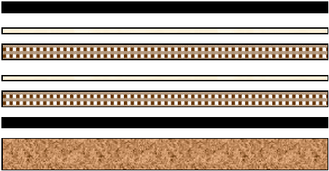
It is important to manually remove the burrs after the routing process so as to prevent damage to the substrate and copper surface, and then use sulfur-free paper for separation purpose.