


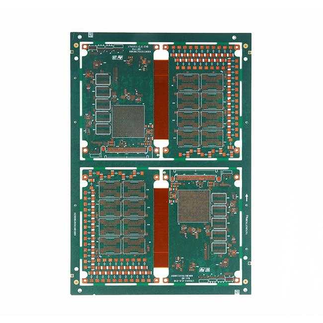
Multi-layer blind buried and blind hole structure printed circuit boards are generally completed by the “sub-board” production method, which means that it must be completed through multiple pressing, drilling, and hole plating, so precise positioning is very important.
The high-precision printed circuit refers to the use of fine line width/spacing, micro holes, narrow ring width (or no ring width), and buried and blind holes to achieve high density. And high precision means that the result of “fine, small, narrow, thin” will inevitably lead to high precision requirements. Take the line width as an example: 0.20mm line width, according to regulations, the production of 0.16-0.24mm is qualified. The error is (0.20 soil 0.04) mm; and the line width of 0.10 mm, the error is (0.10 ± 0.02) mm, obviously the accuracy of the latter is doubled and so forth. This principle is so easy to understand that more discussion is not necessary.
Buried, blind, and through-hole (multi-layer blind-buried circuit boards) combined technology is also an important way to increase the density of printed circuits. Generally, buried and blind via holes are tiny holes. In addition to increasing the number of wiring on the circuit board, the buried and blind via holes are interconnected with the “nearest” inner layer, which greatly reduces the number of holes formed and simplifies the steps of setting up a disk. Thereby this method increasing the number of effective wiring and inter-layer interconnections in the board, and increasing the density of interconnections.
By adopting the pin front positioning system of ordinary multi-layer circuit board production, the graphic production of each layer of single-chip is unified into a positioning system, which creates conditions for successful manufacturing. For the ultra-thick single chip used this time, if the board thickness reaches 2 mm, a certain thickness layer can be milled at the location of the positioning hole, and it is also attributed to the processing of the four-slot positioning hole punching equipment of the front positioning system ability.
XPCB Limited is a premium PCB & PCBA manufacturer based in China.
We specialize in multilayer flexible circuits, rigid-flex PCB, HDI PCB, and Rogers PCB.
Quick-turn PCB prototyping is our specialty. Demanding project is our advantage.
Tel : +86-136-3163-3671
Fax : +86-755-2301 2705
Email : [email protected]
© 2023 - XPCB Limited All Right Reserve
