• +86-755-23012705
  • Building 3, Jinfeng Industrial Park, Fuyong Street, Baoan District, Shenzhen ,China
  • [email protected]
logo
  • Home
  • About Us
    • Flexible PCB Expertise
    • Our Certifications
    • Our Facility
    • Quality Assurance
  • PCB Fabrication
    • Flexible PCB
    • Rigid Flex PCB
    • Rigid PCB
    • ELIC HDI PCB
    • RF PCB
    • Medical PCB
    • Automotive PCB
    • IoT & IIoT PCB
    • Industrial Control PCB
    • Telecommunication PCB
    • Consumer Electronics PCB
  • PCB Assembly
    • Turn Key PCB Assembly
    • Consigned PCB Assembly
    • Components Sourcing
  • Capabilities
    • PCB Fab Capability
    • ATE PCB Fabrication
    • PCB Technology Roadmap
    • PCB Assembly Services
    • PCB Design Support
  • Contact
  • Resources
    • PCB Blog
    • PCB Glossary
Get Quote

What Is The Use Of Solder Mask Opening In PCB Design And How To Design?

I often hear people talk about solder mask opening in PCB design. What is windowing, PCB design windowing what to use, how to open a solder mask? The following is your answer.


What is solder mask opening?

Usually, the leads on the PCB are covered with oil to prevent short circuits and damage to the equipment. The solder mask opening is to remove the coating layer from the wire so that it can be exposed to tin.


What is the use of solder mask opening in PCB design?

PCB design can not only realize the PCB as a plug and play plug-in, but also increase the thickness of solder to achieve the purpose of excessive current.

soldermask opening What Is The Use Of Solder Mask Opening In PCB Design And How To Design?

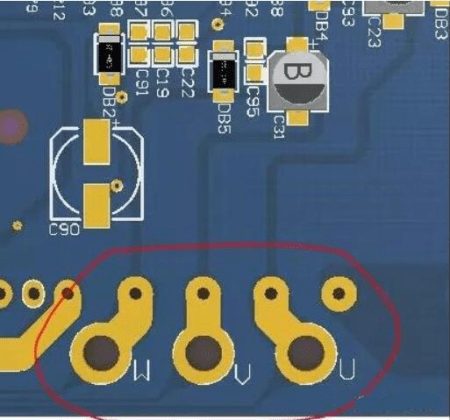
As shown in the figure above, the solder mask opening.

PCB solder mask openings are not uncommon, and one of the most common is likely to be memory chips. Anyone who has taken apart a computer knows that there is a golden finger on the memory strip. In this case, the golden finger is the open solder mask, plug, and play. The solder mask opening also has a very common function, that is, the late iron increases the thickness of the copper foil, which facilitates the excessive current, which is more common on the power board and the motor control board.


How to open solder mask in PCB design?

In PCB design, you can set up threading and solder mask opening on the TOP/BOTTOM SOLDER layer. Top /BOTTOM SOLDER green oil layer: the TOP/BOTTOM SOLDER green oil layer is laid to prevent tin from the copper foil and maintain insulation.

The solder mask green oil can be set at the welding pad, through-hole, and non-electrical wiring of this layer.

  1. The solder pad will open the window by default in PCB design (Override: 0.1016mm), that is, the solder pad will expose copper foil and expand 0.1016mm, and solder will be applied in the wave soldering process. It is recommended that no design changes be made to ensure weldability;
  2. Override: 0.1016mm) in PCB design will open the window, that is, through the hole exposed copper foil, expansion 0.1016mm, wave solder. If the design is to prevent sticking SOLDER to the SOLDER MASK, the PENTING option of the SOLDER MASK must be checked to turn off the SOLDER MASK.
  3. In addition, non-electrical wiring can be carried out separately in this layer so that the green oil can be blocked and the Windows can be opened accordingly. If on copper foil wire, it is used to enhance the ability of the wire to overcurrent. Tin is added during the welding process. If non-copper foil lines are used, typically for logo and special character screen printing, they can be omitted to produce character screen layers.
Share

Related posts

dispensing in PCB
2025-02-07

Multilayer PCB Assembly and HDI PCB Manufacturing for High-Tech Solutions


Read more
smt product line
2025-02-06

Streamline Your PCB Production with XPCB’s Turnkey PCBA Services


Read more
2025-02-05

Comprehensive Turnkey PCBA Services: From BOM to SMT Assembly


Read more
amazon
amphenol-logo
halliburton
intel logo
samtec logo
sanmina logo

Company Info

XPCB Limited is a premium PCB & PCBA manufacturer based in China.

We specialize in multilayer flexible circuits, rigid-flex PCB, HDI PCB, and Rogers PCB.

Quick-turn PCB prototyping is our specialty.  Demanding project is our advantage.

Head Office

XPCB Limited
Address :
Building 3, JinFeng Industry Area,  Fuyong Town, Baoan District, Shenzhen, Guangdong, 518103, China.

Tel : +86-136-3163-3671
Fax : +86-755-2301 2705
Email : [email protected]

Quick Links

  • Flexible PCB
  • Rigid Flex PCB
  • ELIC HDI PCB
  • RF PCB
  • PCB Capability
  • PCBA Capabiility
  • About Us

PCB Blog

Multilayer PCB Assembly and HDI PCB Manufacturing for High-Tech Solutions

Read More »

Streamline Your PCB Production with XPCB’s Turnkey PCBA Services

Read More »

Comprehensive Turnkey PCBA Services: From BOM to SMT Assembly

Read More »

© 2024 - XPCB Limited All Right Reserve