• +86-755-23012705
  • Building 3, Jinfeng Industrial Park, Fuyong Street, Baoan District, Shenzhen ,China
  • [email protected]
logo
  • Home
  • About Us
    • Flexible PCB Expertise
    • Our Certifications
    • Our Facility
    • Quality Assurance
  • PCB Fabrication
    • Flexible PCB
    • Rigid Flex PCB
    • Rigid PCB
    • ELIC HDI PCB
    • RF PCB
    • Medical PCB
    • Automotive PCB
    • IoT & IIoT PCB
    • Industrial Control PCB
    • Telecommunication PCB
    • Consumer Electronics PCB
  • PCB Assembly
    • Turn Key PCB Assembly
    • Consigned PCB Assembly
    • Components Sourcing
  • Capabilities
    • PCB Fab Capability
    • ATE PCB Fabrication
    • PCB Technology Roadmap
    • PCB Assembly Services
    • PCB Design Support
  • Contact
  • Resources
    • PCB Blog
    • PCB Glossary
Get Quote

Method for Double-sided and Multiple-sided Copy Board

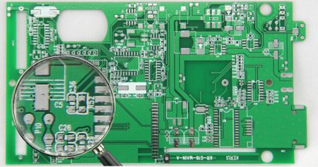
Double-sided Copy Board Method:

  1. Scan the upper and lower layers of the circuit board and save two BMP pictures.
  2. Open the copy board software Quickpcb2005, click “File” and “Open Base Map” to open a scanned picture. Use PAGEUP to zoom in on the screen, see the pad, press PP to place a pad, see the line follow the PT line, just like a child drawing, draw it in this software, click “save” to generate a B2P file.
  3. Click “File” and “Open Base Image” to open another layer of scanned color image.
  4. Click “File” and “Open” again to open the B2P file saved earlier. We see the newly copied board, stacked on top of this picture-the same printed circuit board, the holes are in the same position, but the circuit connections are different. So we press “Options”-“Layer Settings”, turn off the top-level line and silk screen display here, leaving only multi-sidedvias.
  5. The vias on the top layer are in the same position as the vias on the bottom picture. Now you can trace the lines on the bottom layer as you did in childhood. Click “Save” again-the B2P file now has two layers of information on the top and bottom layers.
  6. Click “File” and “Export as PCB File” to get a PCB file with two layers of data. You can change the board or output the schematic diagram or send it directly to the PCB plate factory for production.

Method for Double sided and Multiple sided Copy Board Method for Double-sided and Multiple-sided Copy Board


Multilayer Board Copy Method:

In fact, the four-sided board copying is repeated copying two double-sided boards, and the sixth layer is repeated copying three double-sided boards. The reason why the multi-sided board is daunting is that the internal wiring cannot be seen. How to see the inner layer of a precision multi-sided board?Layering.


There are many methods of layering, such as potion corrosion, tool stripping, etc., but it is easy to separate the layers and lose data. From experience, sanding is the most accurate.

After copying the top and bottom layers of the PCB, sandpaper is usually used to polish the surface layer to show the inner layer; sandpaper is ordinary sandpaper sold in hardware stores. Generally, the PCB is laid flat, and then press the sandpaper and rub evenly on the PCB ( If the board is very small, you can also spread the sandpaper flat, press the PCB with one finger and rub it on the sandpaper). The main point is to pave it flat so that it can be ground evenly.


The silk screen and green oil are generally wiped off, and the copper wire and copper skin should be wiped a few times. Generally speaking, the Bluetooth board can be wiped in a few minutes, and the memory stick will take about ten minutes. Of course, if you have more energy, it will take less time. If you have less energy, it will take more time.

Summary: Understand the above-mentioned six methods of pcb imitation, double-sided and multi-sided board copying methods, these methods introduced above to actually operate correctly, get the same printed circuit board as the original printed circuit board, this time it should be carried out test. If its prototype and performance are exactly the same as the original one.

XPCB Limited is a manufacturer specializing in the production of high-precision double-sided, multi-sided and impedance, blind buried vias, and thick copper circuit boards. The products cover HDI, thick copper, backplanes, rigid-flex, and buried capacitance. Various types of circuit boards such as, Golden Finger, etc. can meet the needs of customers for various products.

Share

Related posts

dispensing in PCB
2025-02-07

Multilayer PCB Assembly and HDI PCB Manufacturing for High-Tech Solutions


Read more
smt product line
2025-02-06

Streamline Your PCB Production with XPCB’s Turnkey PCBA Services


Read more
2025-02-05

Comprehensive Turnkey PCBA Services: From BOM to SMT Assembly


Read more
amazon
amphenol-logo
halliburton
intel logo
samtec logo
sanmina logo

Company Info

XPCB Limited is a premium PCB & PCBA manufacturer based in China.

We specialize in multilayer flexible circuits, rigid-flex PCB, HDI PCB, and Rogers PCB.

Quick-turn PCB prototyping is our specialty.  Demanding project is our advantage.

Head Office

XPCB Limited
Address :
Building 3, JinFeng Industry Area,  Fuyong Town, Baoan District, Shenzhen, Guangdong, 518103, China.

Tel : +86-136-3163-3671
Fax : +86-755-2301 2705
Email : [email protected]

Quick Links

  • Flexible PCB
  • Rigid Flex PCB
  • ELIC HDI PCB
  • RF PCB
  • PCB Capability
  • PCBA Capabiility
  • About Us

PCB Blog

Multilayer PCB Assembly and HDI PCB Manufacturing for High-Tech Solutions

Read More »

Streamline Your PCB Production with XPCB’s Turnkey PCBA Services

Read More »

Comprehensive Turnkey PCBA Services: From BOM to SMT Assembly

Read More »

© 2024 - XPCB Limited All Right Reserve