• +86-755-23012705
  • Building 3, Jinfeng Industrial Park, Fuyong Street, Baoan District, Shenzhen ,China
  • [email protected]
logo
  • Home
  • About Us
    • Flexible PCB Expertise
    • Our Certifications
    • Our Facility
    • Quality Assurance
  • PCB Fabrication
    • Flexible PCB
    • Rigid Flex PCB
    • Rigid PCB
    • ELIC HDI PCB
    • RF PCB
    • Medical PCB
    • Automotive PCB
    • IoT & IIoT PCB
    • Industrial Control PCB
    • Telecommunication PCB
    • Consumer Electronics PCB
  • PCB Assembly
    • Turn Key PCB Assembly
    • Consigned PCB Assembly
    • Components Sourcing
  • Capabilities
    • PCB Fab Capability
    • ATE PCB Fabrication
    • PCB Technology Roadmap
    • PCB Assembly Services
    • PCB Design Support
  • Contact
  • Resources
    • PCB Blog
    • PCB Glossary
Get Quote

Testing Methods for HDI Printed Circuit Board Manufacturirng

To ensure the  quality of HDI printed circuit boards, manufacturers carry out a variety of inspection methods during the production process, and each inspection method will reveal different HDI circuit board defects.

HDI PCB stacking BY xpcb

1. HDI circuit board size and appearance inspection

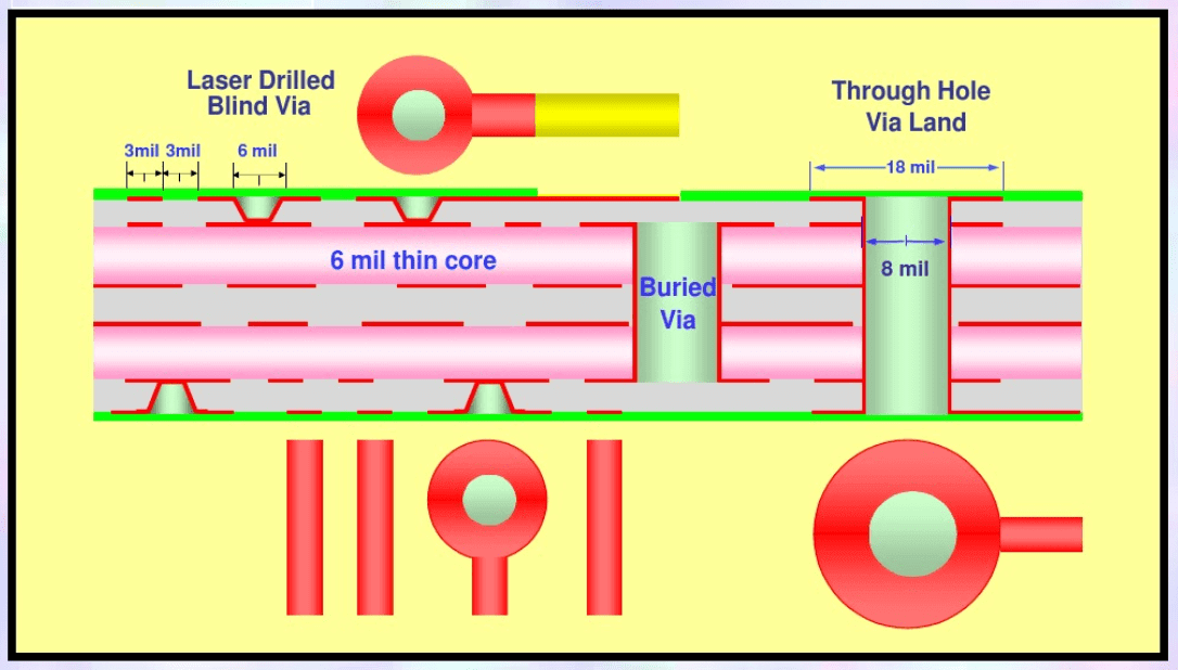
The content of HDI circuit board size inspection mainly includes the directness of processing holes, spacing and tolerances, and the edge size of HDI circuit boards. The content of appearance defect inspection mainly includes: the alignment of the solder mask and the pad; whether the solder mask has abnormal conditions such as impurities, peeling, wrinkles, etc.; whether the reference mark is qualified; whether the circuit conductor width (line width) and spacing are in line Requirements; Whether the multilayer board is peeled off, etc. In practical applications, special equipment for HDI circuit board appearance testing is often used to detect it. Typical equipment is mainly composed of computers, automatic workbenches, and image processing systems. This system can detect the inner and outer layers of the multilayer board, single/dual panels, and base map films; it can detect broken lines, overlapping lines, scratches, pinholes, line widths, rough edges, and large Area defects, etc.

2. HDI circuit board solder mask integrity test

HDI circuit boards generally use dry film solder mask and optical imaging solder mask. These two kinds of solder mask have high resolution and immobility. Dry film solder mask is laminated on the PCB under the action of pressure and heat. It requires a clean HDI circuit board surface and an effective lamination process. This kind of solder mask tin-lead alloy has poor surface adhesion. Under the impact of thermal stress generated by reflow soldering, the phenomenon of peeling and breaking from the surface of the HDI circuit board often occurs. This kind of solder mask is also relatively brittle, and may cause micro-cracks under the influence of heat and mechanical force during leveling. In addition, physical and chemical damage may also occur under the action of cleaning agents. In order to find out these potential defects of dry film solder mask, strict thermal stress tests should be performed on HDI circuit boards during incoming material inspection. When the solder mask peeling is not observed during the test, the HDI circuit board test piece can be immersed in water after the test, and the capillary action of the water between the solder mask and the PCB surface is used to observe the solder mask peeling. It is also possible to immerse the HDI circuit board specimen in the SMA cleaning agent after the test to observe whether it has physical and chemical effects with the solvent.
Thank you for your reading. XPCB Limited is a professional PCB & PCBA manufacturer based in China, offer high-quality rigid PCB,   flexible circuit,  rigid-flex PCB,  HDI PCB,  Rogers PCB fabrication service. If you need PCB prototype quote, just contact us here [email protected]. 
Share

Related posts

dispensing in PCB
2025-02-07

Multilayer PCB Assembly and HDI PCB Manufacturing for High-Tech Solutions


Read more
smt product line
2025-02-06

Streamline Your PCB Production with XPCB’s Turnkey PCBA Services


Read more
2025-02-05

Comprehensive Turnkey PCBA Services: From BOM to SMT Assembly


Read more
amazon
amphenol-logo
halliburton
intel logo
samtec logo
sanmina logo

Company Info

XPCB Limited is a premium PCB & PCBA manufacturer based in China.

We specialize in multilayer flexible circuits, rigid-flex PCB, HDI PCB, and Rogers PCB.

Quick-turn PCB prototyping is our specialty.  Demanding project is our advantage.

Head Office

XPCB Limited
Address :
Building 3, JinFeng Industry Area,  Fuyong Town, Baoan District, Shenzhen, Guangdong, 518103, China.

Tel : +86-136-3163-3671
Fax : +86-755-2301 2705
Email : [email protected]

Quick Links

  • Flexible PCB
  • Rigid Flex PCB
  • ELIC HDI PCB
  • RF PCB
  • PCB Capability
  • PCBA Capabiility
  • About Us

PCB Blog

Multilayer PCB Assembly and HDI PCB Manufacturing for High-Tech Solutions

Read More »

Streamline Your PCB Production with XPCB’s Turnkey PCBA Services

Read More »

Comprehensive Turnkey PCBA Services: From BOM to SMT Assembly

Read More »

© 2024 - XPCB Limited All Right Reserve