


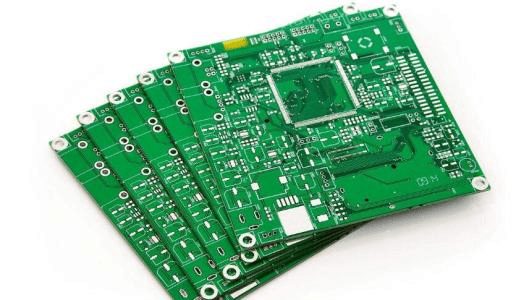
PCB vias are an important part of the multilayer circuit board, and the types of PCB vias are divided into three types: blind vias, buried vias, and through vias.
The difference between the three vias
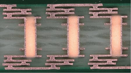
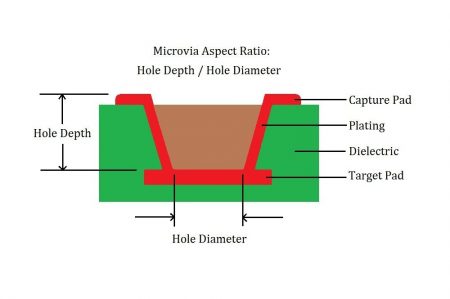
(1) Blind hole: Located on the top and bottom surface of the circuit board, with a certain depth, used for the connection of the surface line and the inner layer of the inner line, the depth of the hole and the hole diameter usually do not exceed a certain ratio.
(2) Buried via: The connecting hole located in the inner layer of the board will not extend to the surface layer of the PCB board. Blind holes and buried holes are in the inner layer of the circuit board, and the required through holes are drilled before lamination, and the through holes drilled before lamination become inner holes, which mostly appear in multi-layer circuit boards, and double-sided panels will not appear in this situation.
(3) Through hole: Penetrates from the bottom of the layer to the top layer, and can be used to realize internal interconnection or as a mounting positioning hole for components. Because through-holes are easier to implement in the process and less costly, through-holes are generally used in printed circuit boards.
Advantages of blind and buried vias
The application of blind and buried holes can reduce the size and number of layers of the circuit board to a certain extent, improve electromagnetic compatibility, reduce the cost of customization, increase product characteristics, and the wiring space occupied by through holes is very large.
If a large number of through-holes are densely packed into one piece, it will bring obstacles to the inner wiring of the multi-layer circuit board, and when it densely passes through the surface of the power park and the ground layer, it will not only destroy the impedance characteristics of the power ground layer, but also make the power ground layer fail.
Of course, the specific design of vias depends on the customer’s product requirements, and not all multilayer circuit boards need to be used for blind or buried vias.
Simplify Your PCB Journey with XPCB Limited
XPCB Limited simplifies the PCB process for you. With our quick-turnaround prototyping and turnkey PCBA services, we ensure that your projects move forward smoothly and efficiently. Trust our commitment to quality and timeliness as we help you bring your designs to life. Choose XPCB Limited for a hassle-free PCB experience.
XPCB Limited is a premium PCB & PCBA manufacturer based in China.
We specialize in multilayer flexible circuits, rigid-flex PCB, HDI PCB, and Rogers PCB.
Quick-turn PCB prototyping is our specialty. Demanding project is our advantage.
Tel : +86-136-3163-3671
Fax : +86-755-2301 2705
Email : [email protected]
© 2023 - XPCB Limited All Right Reserve
