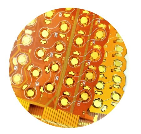
4oz Flex PCB for EV BMS
Explore this outstanding 4oz heavy copper flex PCB built for the EV Battery Management System application, featuring heavy copper thickness and large size.
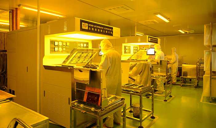
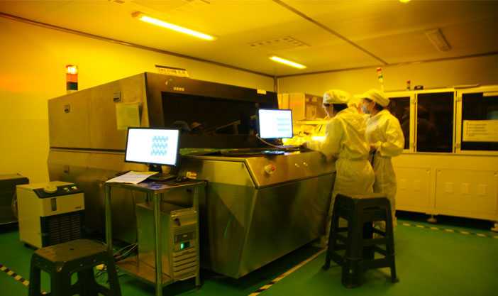
Flexible circuit manufacturing involves much fewer fab steps compared to rigid PCB, here introduce them briefly.
1. Adhesive/Seed finishing applied
Either an epoxy or acrylic adhesive is used, or sputtering is used to create a thin copper layer for a plating key.
2. Copper foil added.
Copper foil is included, either by lamination to the glue (the a lot more mainstream approach) or chemical plating onto the seed layer. Newer construction processes by products suppliers permit adhesiveless lamination of rolled stiff copper as a choice.
3. Drilling
Openings to vias and pads are frequently mechanically pierced. Several plated flex substrates can be drilled concurrently by incorporating them from several reels on drums, exploration in between working plates, after that rolling out to separate reels on the other side of the drilling maker. Pre-cut flex panels can be combined as well as pierced in between rigid blanks similarly inflexible cores are pierced too, though it calls for more careful registration and the alignment accuracy is reduced. For ultra-small openings, laser drilling is readily available, though at a lot included cost due to the fact that each film needs to be drilled independently. This would certainly make use of Excimer (ultraviolet) or YAG (Infrared) lasers for higher accuracy (microvias), as well as CO2 lasers for tool openings (4+ mils). Huge openings and also cut.
4.Through-hole plating.
When the holes are made, copper is transferred and also chemically plated similarly as stiff PCB cores.
( typically described as Cuposit). Through-hole layering in flex circuits is suggested to be at the very least.
1 mil in layering density to add mechanical support to the pad or through, whereas a typical low-cost rigid PCB may just have 1/2 mil cuposit.
5.Etch-resist printing.
Photosensitive etch withstand is covered onto the movie surface areas, and also the desired mask pattern is used to reveal and establish the stand up to before chemical etching of the copper .
6. Etching as well as stripping.
After exposed copper is etched, the etch stand up to is chemically removed from the flex circuit.
7. Coverlay or Covercoat.
Leading as well as bottom areas of the flex circuit are shielded by coverlay layers which are reduced to shape. There may be parts really installed on sections of the adaptable circuit, in which instance the coverlay is likewise acting as a solder mask. The most usual coverlay product is additional polyimide film with sticky though adhesiveless processes are available. In the adhesiveless process, photoimageable solder mask ( the like used on inflexible board sections) is made use of basically printing the coverlay onto the flex circuit. For coarser cheaper layouts display printing is also a choice with final healing of this cover coat film by UV exposure. Basically, the difference is that coverlay is a laminated film, whereas covercoat is a used product finishing which then requires to be cured.
8. Cutting out the flex.
The final step in creating the flex circuit is cutting it out. This is usually described as
” blanking”. The high-volume cost-effective approach to blanking is by a hydraulic strike
as well as die set which includes fairly high tooling costs. However, this method permits punching out of lots of flex circuits at the exact same
time. For prototype and low-volume runs, a blanking knife is made use of. The blanking blade is basically a lengthy razor blade, bent right into the form of the flex circuit outline as well as fastened right into a directed slot in a support board (MDF, plywood or thick plastic such as teflon). The flex circuits are after that pressed right into the blanking knife to be cut out. For also smaller sized prototype runs, X/Y cutters (similar to those used in vinyl indicator making) could be utilized.

Explore this outstanding 4oz heavy copper flex PCB built for the EV Battery Management System application, featuring heavy copper thickness and large size.
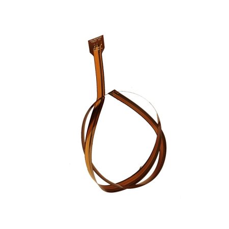
This is an 1100mm length flex PCB made of polyimide material with ENIG. x-pcb.com is a long flexible circuit and Polyimide Flex PCB manufacturer in china on your demand for flexible printed circuit boards.
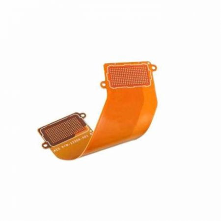
A 10 Layers Flexible PCB made by XPCB, built for a top-class flex PCB connector. We are one of the best flex PCB manufacturers in China, offering turnkey flex PCB assembly service.
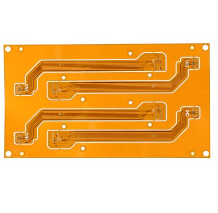
Flex PCB Prototype Manufacturer | Quick-turn Flexible PCB Prototyping XPCB™ INTRO XPCB Limited was founded with a focus on providing high-quality flex PCB prototyping services. We
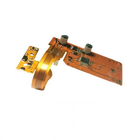
XPCB Ltd offers a one-stop FPC+Component sourcing+ assembly service to global customers. Our top-notch flexible PCB fabrication and flexible PCB assembly services include SMT and DIP. If you are looking for a quick-turn flexible PCBA service provider, then trust our experienced team of flex PCB assembly manufacturers and suppliers to deliver high-quality, and reliable results.Don’t hesitate to call us or email [email protected].
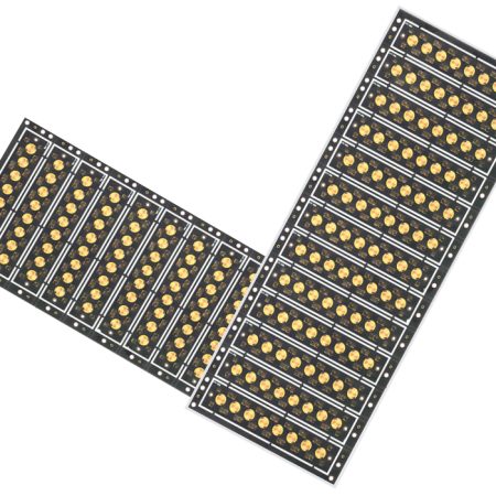
An doubled-side flexible PCB prototype made by x-pcb.com, it comes with 3u” Electroplated Gold finish. If you have similar flex PCB quote needed, contact us now! We are an professional flex PCB manufacturer from China.


XPCB Limited is a premium PCB & PCBA manufacturer based in China.
We specialize in multilayer flexible circuits, rigid-flex PCB, HDI PCB, and Rogers PCB.
Quick-turn PCB prototyping is our specialty. Demanding project is our advantage.
Tel : +86-136-3163-3671
Fax : +86-755-2301 2705
Email : [email protected]
© 2023 - XPCB Limited All Right Reserve
