• +86-755-23012705
  • [email protected]
  • Building 3, Jinfeng Industrial Park, Fuyong Street, Baoan District, Shenzhen ,China
Search
Close
logo
  • Home
  • About Us
    • About XPCB
    • Flexible PCB Fabrication
    • PCB Fab Capability
    • PCBA Capability
    • Our Certifications
    • Our Facility
    • Quality Assurance
  • PCB Fabrication
    • Flexible PCB
    • Rigid Flex PCB
    • Rigid PCB
    • ELIC HDI PCB
    • RF PCB
    • Medical PCB
    • Automotive PCB
    • IoT & IIoT PCB
    • Industrial Control PCB
    • Telecommunication PCB
    • Consumer Electronics PCB
  • PCB Assembly
    • Turn Key PCB Assembly
    • Consigned PCB Assembly
    • Components Sourcing
  • Resources
    • PCB Glossary
    • PCB Design Guide
    • PCB Blog
  • Contact
Menu
  • Home
  • About Us
    • About XPCB
    • Flexible PCB Fabrication
    • PCB Fab Capability
    • PCBA Capability
    • Our Certifications
    • Our Facility
    • Quality Assurance
  • PCB Fabrication
    • Flexible PCB
    • Rigid Flex PCB
    • Rigid PCB
    • ELIC HDI PCB
    • RF PCB
    • Medical PCB
    • Automotive PCB
    • IoT & IIoT PCB
    • Industrial Control PCB
    • Telecommunication PCB
    • Consumer Electronics PCB
  • PCB Assembly
    • Turn Key PCB Assembly
    • Consigned PCB Assembly
    • Components Sourcing
  • Resources
    • PCB Glossary
    • PCB Design Guide
    • PCB Blog
  • Contact
Get Instant Quote
Show all
HDI 2 stacking

HDI Printed Circuit Board Overview

Categories: ELIC HDI PCB, PCB Fabrication
Share
  • Description

What Is HDI Printed Circuit Board?

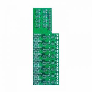
High-density interconnect, or HDI, circuit boards are printed circuit boards with a higher wiring density per unit area than traditional printed circuit boards. In general, HDI PCBs are defined as PCBs with one or all of the following: microvias; blind and buried vias; built-up laminations and high signal performance considerations. Printed circuit board technology has been evolving with changing technology that calls for smaller and faster products. HDI boards are more compact and have smaller vias, pads, copper traces and spaces. As a result, HDIs have denser wiring resulting in lighter weight, more compact, lower layer count PCBs. Rather than using a few PCBs in a device, one HDI board can house the functionality of the previous boards used.


Structure of HDI Circuit Board

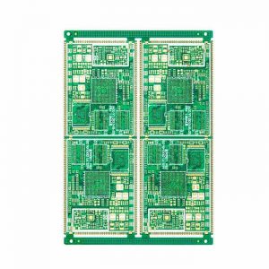
-HDI PCB (1+N+1): Simplest HDI

  • This structure of HDI PCB contains 1 “build-up” of high-density interconnection layers, suitable for BGA with lower I/O counts.
  • It has fine lines, microvia and registration technologies capable of 0.4 mm ball pitch, excellent mounting stability and reliability, and may contain copper filled via.
  • Applications: Cell phone, MP3 Player, GPS, Memory Card.

Fig1: 1+N+1 HDI PCB

HDI 1 stacking HDI Printed Circuit Board Overview


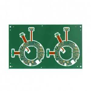
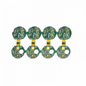
-HDI PCB (2+N+2): Moderate Complex HDI

  • This structure of HDI PCB contains 2 or more “build-up” of high-density interconnection layers; microvias on different layers can be staggered or stacked; Copper filled stacked microvia structures are commonly seen in challenging designs that demand high level signal transmission performance.
  • These are suitable for BGA with smaller ball pitch and higher I/O counts and can be used to increase routing density in a complicated design while maintaining a thin finished board thickness.
  • Applications: Cell phone, PDA, game console, portable video recording devices.

Fig2:  2+N+2 HDI PCB

HDI 2 stacking HDI Printed Circuit Board Overview


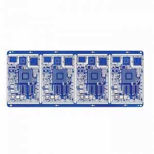
-ELIC (Every Layer Interconnection): Most Complex HDI

  • In this HDI PCB structure, all the layers are high-density interconnection layers which allow the conductors on any layer of the PCB to be interconnected freely with copper filled stacked microvia structures.
  • This provides a reliable interconnect solution for highly complex large pin-count devices, such as CPU and GPU chips utilized on handheld and mobile devices while producing superior electrical characteristics.
  • Applications: Cell phone, ultra-mobile PC, MP3, GPS, Memory cards, small computer devices.


What Advantages HDI PCB Has Versus Other PCB Types?

  • Phenomenal versatility: HDI boards are ideal where weight, space, reliability, and performance are primary concerns.
  • Compact design: The combination of blind vias, buried vias, and microvias brings down the board space requirement.
  • Better signal integrity: HDI incorporates via-in-pad and blind via technology. This helps in placing the components closer to each other which cuts down the signal path length. It therefore remarkably improves signal integrity due to shorter signal paths.
  • High reliability: The implementation of stacked vias make these boards a super shield against extreme environmental conditions.
  • Cost-effective: The functionality of a standard 8-layer through-hole board (standard PCB) can be reduced to a 4-layer HDI board without compromising the quality.


Applications of HDI Printed Circuit Board

  • Smartphones and Tablets

All smartphones are HDI PCBs with ELIC (Every Layer Interconnection) construction. The HDI PCBs are responsible for creating thinner are smaller portable electronic devices.

  • Wearable Technology

With the launch of Apple watch and other wearable devices like VR headsets, HDI is becoming the major stakeholder in the consumer market.

  • Healthcare

The HDI PCB is making an impact on the medical industry. The medical devices are usually HDI since they can fit in small devices like implants and lab and imaging equipment.

  • Telecom

As 5G technology is set to jump start since 2020, the demand for more versertile and advanced PCBs grow rapidly.  HDI PCB’s super connectivity allows wide employmet of  5G technology  become possible.

  • Automotive 

Like almost everything else, cars are becoming more connected and computerized. Today’s cars have around 50 microprocessors on board that play a role in engine controls, diagnostics, safety features and other conveniences. Many advanced features such as onboard WiFi and GPS, rearview cameras and backup sensors rely on HDI PCBs. As automotive technology continues to advance, HDI tech will likely play an increasingly important role.


HDI PCB Fabrication Process 

HDI PCB PROCESS HDI Printed Circuit Board Overview


Why Choose XPCB as Your HDI PCB Supplier?

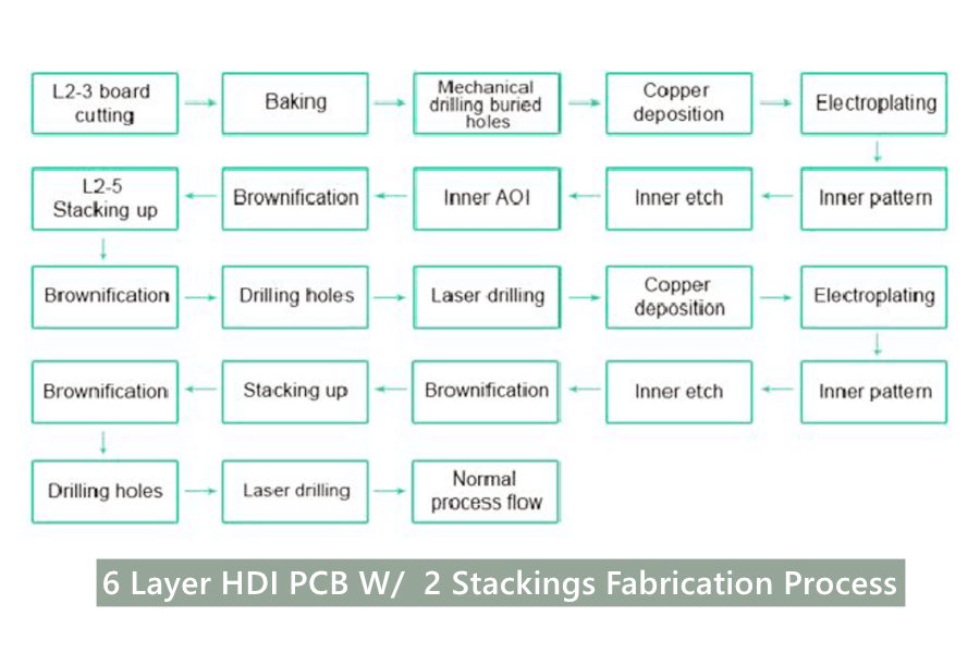
Equipped with up-to-date Laser drilling machine, XPCB is able to cope with most complex HDI structure-ELIC in decent manner, without the high scrappage rate due to conventional mechnical drilling method.  We adopt strict quality inspection standards,  using IPC-6016, IPC-6011,IPC-6012,IPC-4104, IPC-TM-650 as validating documents. Careful DFM checking will be performed before production.  Any suggestion that will help refine the stackup or bring down cost will be updated to customer in details free of charge.


HDI PCB quote request HDI Printed Circuit Board Overview


PRODUCT ENQUIRE

    RELATED PRODUCTS

    • Flexible PCB Prototyping

      6 Layer HDI Flex PCB- High Density Interconnect(HDI) PCB Manufacturer China

    • Base station sub board Base station sub board

      Base station sub board

    • 700 rigid flex pcb 8 Rigid Flex PCB Overview

      Rigid Flex PCB Overview

    • 6 layer HDI Rigid Flex PCB made of FR4 and PI

      6 Layer HDI Rigid Flex PCB

    • 26 LAYERS IMMERSION GOLD BOARD

      IC testing instrument Rigid PCB

    • polyimide Flexible Printed Circuit Board Factory

      Flexible Printed Circuit Board Overview

    • 1100mm long flex pcb manufacturer

      1100mm Long Flex PCB

    • Navigation-module-board

      GPS Module Rigid Flex PCB

    • Automotive entertainment system PCB

      Automotive Entertainment System PCB

    • Home
    • About Us
    • PCB Fabrication
    • PCB Assembly
    • Resources
    • Contact

    Product Category

    • PCB Assembly
    • PCB Fabrication
      • Automotive PCB
      • Consumer Electronics PCB
      • ELIC HDI PCB
      • Flexible PCB
      • Industrial Control PCB
      • IoT & IIoT PCB
      • Medical PCB
      • RF PCB
      • Rigid Flex PCB
      • Rigid PCB
      • Telecommunication PCB
    amazon
    amphenol-logo
    halliburton
    intel logo
    samtec logo
    sanmina logo
    Previous
    Next

    Company Info

    XPCB Limited is a premium PCB & PCBA manufacturer based in China.

    We specialize in multilayer flexible circuits, rigid-flex PCB, HDI PCB, and Rogers PCB.

    Quick-turn PCB prototyping is our specialty.  Demanding project is our advantage.

    Head Office

    XPCB Limited
    Address :
    Building 3, JinFeng Industry Area,  Fuyong Town, Baoan District, Shenzhen, Guangdong, 518103, China.

    Tel : +86-136-3163-3671
    Fax : +86-755-2301 2705
    Email : [email protected]

    Quick Links

    • Flexible PCB
    • Rigid Flex PCB
    • ELIC HDI PCB
    • RF PCB
    • PCB Capability
    • PCBA Capabiility
    • About Us

    PCB Blog

    Electromagnetic Compatibility Design of Mobile Phone PCB (1)

    Read More »

    The PCB Circuit Design of LED Switching Power Supply

    Read More »

    Electromagnetic Compatibility Design of Mobile Phone PCB (2)

    Read More »

    © 2023 - XPCB Limited All Right Reserve