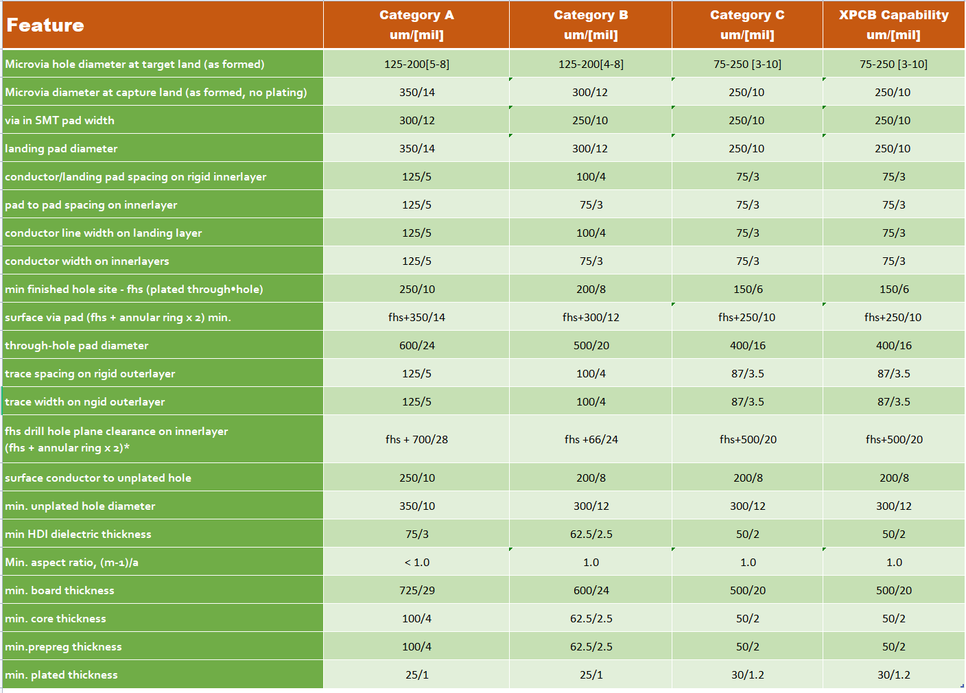
High density interconnected (HDI) PCB, represent one of the fastest-growing technologies in PCBs. Because of its higher circuitry density than traditional circuit boards, the HDI PCB design is able to incorporate smaller vias and capture pads, and higher connection pad densities.
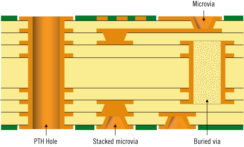
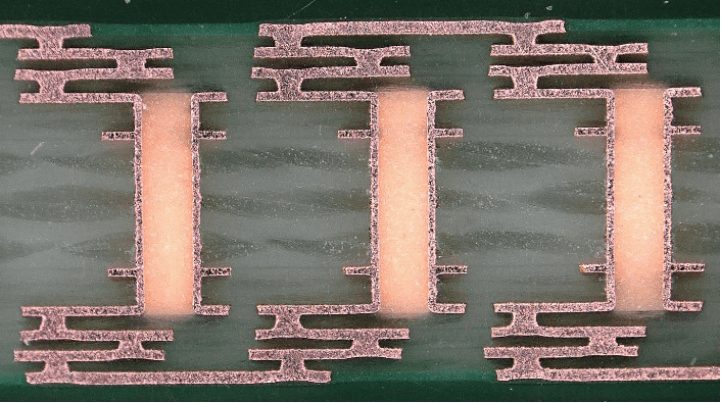
High-Density Interconnects PCB (HDI PCB), also referred as sequential build-up (SBU), and build-up multilayer (BUM) are featured by very small blind, buried, and through vias made by techniques other than mechanical drilling.
The use of more complex components with very high input/output (I/O) counts has pushed the HDI board fabricator to enhance techniques for creating smaller vias, therefore many new or redeveloped processes appeared on the market.They all allow the designer to increase significantly routing density through the use of vias in surface-mount technology (SMT) pads, to reduce the size and weight of the product, and to improve the electrical performance of the system. These types of boards are generically called high-density interconnects (HDI). An HDI board typically will have, as on average, over 110 to 130 electrical connections per square inch (20 connections per sq. cm) on both sides of the board.
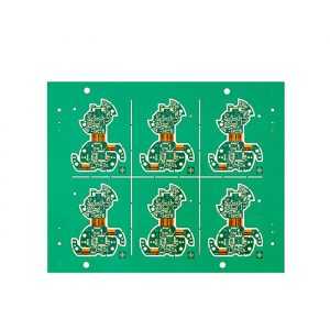
We fabricate a variety of HDI PCB, including rigid HDI PCB, HDI flex PCB, or any PCB with microvia, stacked via, blind via, and buried via. Normally we start by building the prototype, then go to series production. Max layer for HDI PCB manufacturing is 20L.
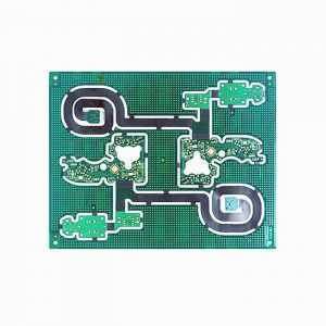
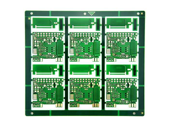
Layer:6L 2 Tier
Thickness:1.3mm
Size:118.29mm*113.12mm
Min blind vias:0.1mm
Min buried vias:0.2mm
Min Trace:0.084mm
Min Space:0.089mm
Finish:ENIG+OSP
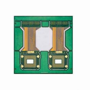
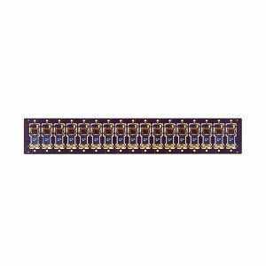
 Layer:4L 1 Tier
Thickness:0.8mm
Size:70mm*86mm
Min Trace:0.12mm Min Space:0.075m
Min Hole Size:0.1m
Finish:ENIG+0SP
Application: Smart Watch
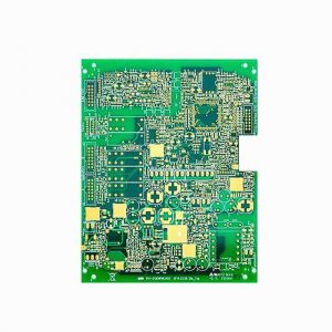
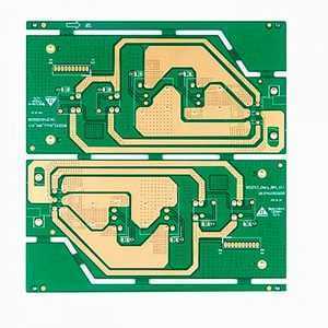
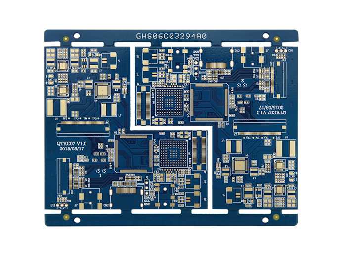 Layer:6L 2 Tier
Thickness:1.0mm
Size:92mm*118mm
Min Trace:0.075mm
Min Space:0.075mm
Min Hole:0.1mm
Finish:ENIG
Application: Mobile Phone
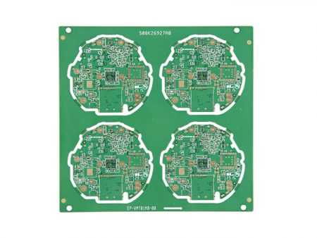
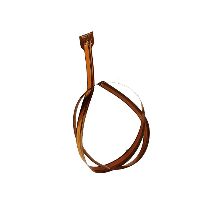
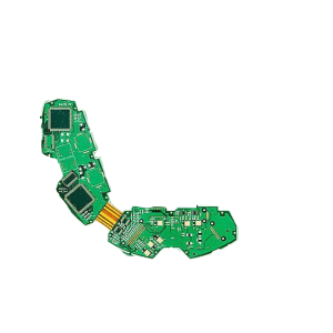
Layer:8L 2 Tier
Thickness:1.0mm
Size:118.29mm*113.12mm
Min blind vias:0.1mm
Min buried vias:0.2mm
Min Trace:0.084mm
Min Space:0.089mm
Finish:ENIG+OSP
Application: Car DVR
We fabricate high-reliability HDI PCB for global customers, both quick-turn prototype and series production. Learn more about our capability below:


XPCB Limited is a premium PCB & PCBA manufacturer based in China.
We specialize in multilayer flexible circuits, rigid-flex PCB, HDI PCB, and Rogers PCB.
Quick-turn PCB prototyping is our specialty. Demanding project is our advantage.
Tel : +86-136-3163-3671
Fax : +86-755-2301 2705
Email : [email protected]
© 2023 - XPCB Limited All Right Reserve